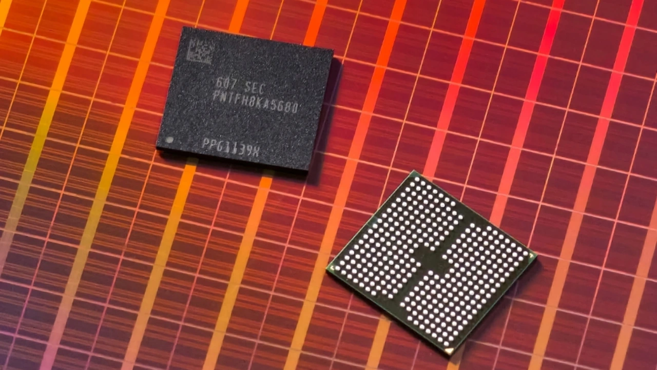
At Future of Memory and Storage (FMS) 2026 in Santa Clara on August 5, Samsung Electronics unveiled concept models for two new 3D memory architectures, Samsung zHBM and zNAND-O, along with an industry-first V10 BV-NAND chip packing more than 400 layers, all aimed at solving one core problem: AI accelerators sitting idle while they wait for data to arrive.
Samsung AI memory showcased two next-generation 3D memory architectures – zHBM and zNAND-O – alongside its industry-first V10 BV-NAND chip featuring more than 400 layers. These AI models are expected to reduce data movement delays, improve energy efficiency, and create faster memory systems for future AI workloads.
Millions Spent, Zero Progress: Why Your AI Accelerators Are Constantly Starving
Anyone who’s watched a high-end graphics card stall while an asset loads knows the frustration of powerful hardware waiting on slow data delivery.
The same bottleneck is playing out at massive scale in AI data centers; companies are spending billions on AI accelerators that end up starved for data because the path between storage and compute hasn’t kept pace with processing power.
Samsung’s FMS 2026 announcements target that exact gap with a shift toward vertical, 3D-stacked memory design.
Out With the Old: Why Side-by-Side Memory Is Officially Dead for AI
What is Samsung zHBM?
Conventional HBM sits beside the AI processor on the same package. zHBM flips that layout, stacking memory directly on top of the AI accelerator instead.
Samsung says this cuts the physical distance data has to travel between processor and memory, which is designed to boost bandwidth and improve power efficiency for large-scale AI training and inference.
Why does the distance matter?
Placing memory right on top of the processor is the difference between data traveling across a package versus barely moving at all.
Less physical distance means less time and energy spent moving data back and forth, which is exactly where a lot of AI system slowdown comes from today. This potentially improves AI workload performance, Bandwidth performance, Power efficiency, and data transfer speed.
The numbers Samsung is claiming
| Metric | zHBM vs. HBM5 |
| Performance | ~8x higher |
| Memory density | 10x+ higher |
| Energy efficiency | 3x better |
| Thermal resistance | Reduced by more than half |
Lower thermal resistance matters because it reduces heat buildup, which in turn reduces performance throttling under heavy load.
Sky-High Storage: Inside Samsung’s Groundbreaking 400+ Layer V10 BV-NAND
Breaking the layer ceiling
Samsung’s V10 BV-NAND uses a new Bonding V-NAND architecture with more than 400 layers, built using wafer bonding technology to stack memory cells.
The announcement comes 13 years after Samsung introduced the industry’s first V-NAND at the 2013 Flash Memory Summit.
What the density gain means
V10 BV-NAND increases memory density by roughly 58% over the previous generation (V9), while also improving read, write, and I/O performance.
In practice, that means more data, whether massive AI models or large datasets, can be stored and accessed faster, cutting down bottlenecks during high-capacity workloads.
zNAND-O for High-Speed Storage to Edge AI
Alongside V10 BV-NAND, Samsung previewed zNAND-O, a high-performance NAND concept built on V-NAND technology and in development in four- and eight-layer versions.
It’s designed for edge AI environments, bringing low-latency, high-efficiency storage closer to local devices rather than only centralized server farms.
Are Samsung’s AI Concepts Ready for Prime Time?
zHBM and zNAND-O are concept models, not shipping products. Samsung is previewing a technical direction, not something available for purchase today.
V10 BV-NAND is the more concrete announcement, alongside real product lines Samsung is already shipping or sampling, including Samsung HBM4E samples sent to customers in May, and enterprise storage like the PM1763.
This is data-center infrastructure aimed at AI training and inference workloads, not consumer gaming hardware.
Whether the vertical-stacking techniques behind zHBM eventually influence consumer memory standards isn’t something Samsung addressed in this announcement; that would be speculation rather than a confirmed roadmap item.
Samsung’s Advantage in the AI Memory Race
Samsung has already begun mass-producing HBM4 using its 1c DRAM and 4nm base die technology, and started shipping HBM4E samples in May 2026. As the only integrated device manufacturer spanning memory, foundry, and advanced packaging, Samsung is positioning itself to move these concepts from lab preview to production faster than competitors relying on outside partners for each piece of the stack.
Can Samsung Turn Next-Gen Memory Dreams Into Reality?
Samsung’s pitch at FMS 2026 is a shift from spreading memory and processors side by side to stacking them vertically, cutting the physical distance data has to travel.
With Samsung AI systems zHBM, zNAND-O, and V10 BV-NAND, the company focuses on vertically stacked memory architectures that will become a key part of next-generation AI infrastructure.
Whether that translates into faster AI systems in production depends on how quickly these concept designs move from prototype to shipping hardware.