
Like a spark igniting a new circuitry of ambition, Odisha steps onto the map of tomorrow’s technology.
A Historic Leap in India’s Chip Journey
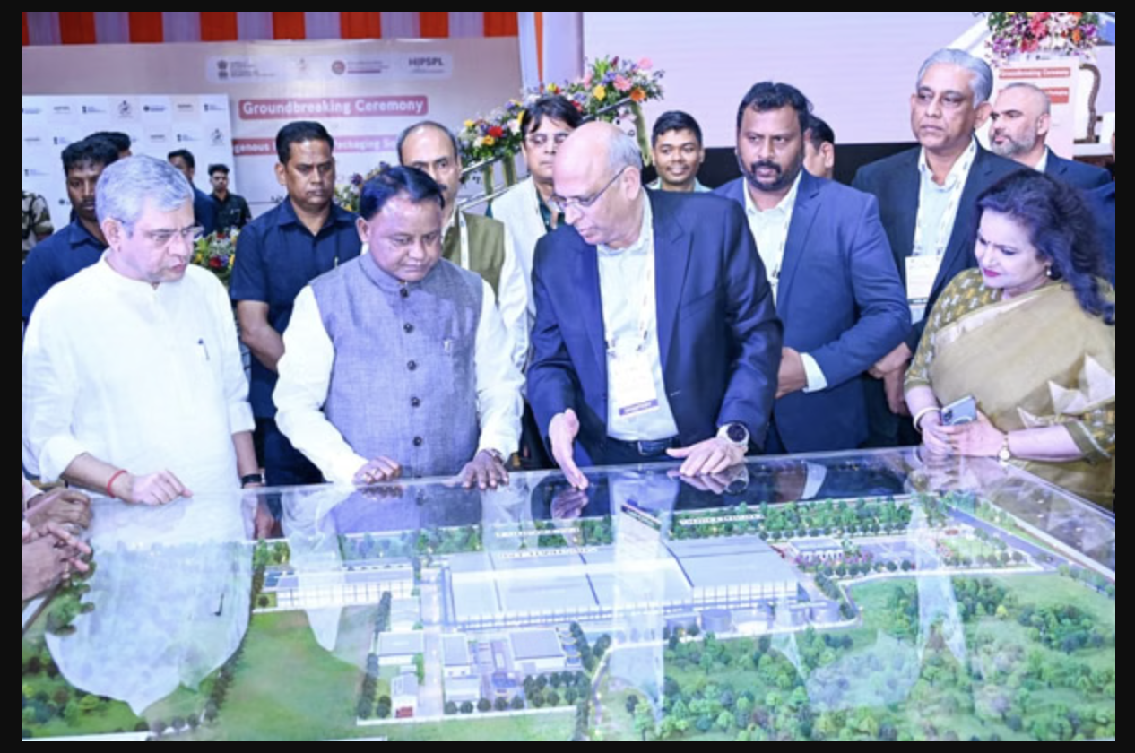
In a landmark development, the foundation stone for India’s first advanced 3D chip packaging unit was laid at Info Valley in Bhubaneswar, Odisha. The project marks a major stride in strengthening the country’s semiconductor ecosystem and aligns with the broader vision of Atmanirbhar Bharat in high-end electronics manufacturing.
Union Minister for Electronics & IT Ashwini Vaishnaw highlighted the significance of the moment, noting that the foundation stone was laid on the auspicious occasion of Akshay Tritiya. He described the project as a proud milestone for Odisha, emphasizing its use of next-generation 3D glass substrate technology in chip manufacturing—an upgrade from the conventional silicon-based approach.
“On the occasion of Akshay Tritiya, the foundation stone of a semiconductor plant has been laid in Odisha. I want to thank PM Modi and CM Mohan Charan Majhi. A high-tech industry coming to Odisha is a matter of pride. This is an advanced technology. Normally, a silicone substrate is used in the manufacturing of chips, and now the technology of advanced 3D Glass substrate will be used, and the foundation stone of the first major plant using that technology has been laid in Odisha,” he said.
He further added, “We will also work to double the capacity of the plant after the completion of the first phase of the plant. Several railway projects are underway in Odisha currently. Railway Stations in Puri, Bhubaneswar, Cuttack and other cities are being redeveloped.”
Powering the Future with Technology and Jobs
Odisha Chief Minister Mohan Charan Majhi called the initiative a historic milestone for both the state and the nation. He noted that this is the first time India will host an advanced 3D glass solutions semiconductor project, reinforcing Odisha’s growing reputation as a technology and manufacturing hub.
The project involves an investment of nearly ₹2,000 crore and is expected to produce 70,000 glass panels annually, along with 50 million assembled units and around 13,000 advanced 3DHI modules. It will also generate employment for over 2,500 people. Majhi emphasized that Odisha is uniquely positioned as the only state hosting both India’s first compound semiconductor fabrication unit and this cutting-edge 3D packaging facility.
He also pointed out that the involvement and interest of global technology leaders such as Intel, Lockheed Martin, and Applied Materials reflect Odisha’s rising industrial prominence.
“This is happening for the first time in the country, and its construction will take place right here in Odisha. This is the future of semiconductor technology. This company is investing Rs 2000 crore in the first phase in Odisha. More than 2500 people will also get employment from this.”
From the soil of Bhubaneswar rises not just a plant, but a blueprint for India’s silicon-powered future.
Summary
India’s first advanced 3D chip packaging unit is being set up in Bhubaneswar, Odisha, marking a major boost to the semiconductor ecosystem. With ₹2,000 crore investment, the project will use next-gen 3D glass substrate technology, generate 2,500+ jobs, and strengthen Atmanirbhar Bharat goals. It positions Odisha as a key hub for future-ready electronics manufacturing.
Image Source
Comments are closed.