
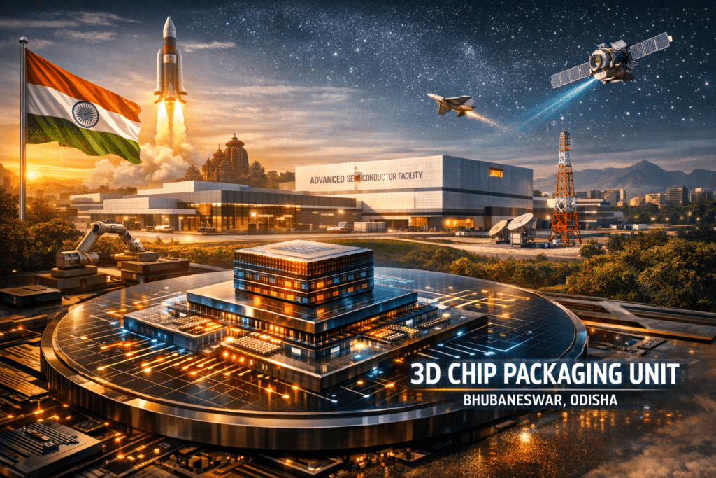
Odisha will break ground on India’s first advanced 3D chip packaging unit on April 19, marking a historic milestone in the country’s semiconductor journey.
The project, titled Heterogeneous Integration Packaging Solutions (3D Glass Solutions)positions Odisha at the forefront of global semiconductor innovation.
Chief Minister Mohan Charan Majhi will lead the ceremony in Bhubaneswar, joined by Union Electronics & IT Minister Ashwini Vaishnaw and Odisha’s Electronics & IT Minister Dr Mukesh Mahaling. Senior officials, global industry leaders, investors, and academic representatives will also attend.
The project introduces glass substrate-based advanced semiconductor packaging technology, making Odisha the first state in India to host both a compound semiconductor fabrication unit and a 3D chip packaging facility. The initiative reflects rapid progress, with groundbreaking scheduled within months of Union Cabinet approval.
Officials confirmed a project outlay of Rs 1,943 crore and an annual production capacity of 50 million assembled units. The facility will generate around 2,500 direct and indirect jobs, strengthening Odisha’s high-tech ecosystem.
The chips produced will serve critical sectors, including aerospace, defence, artificial intelligence, 5G technologies, and data centres. The government emphasised that the project aligns with the vision of Atmanirbhar Bharatboosting India’s self-reliance in advanced electronics.
Comments are closed.