
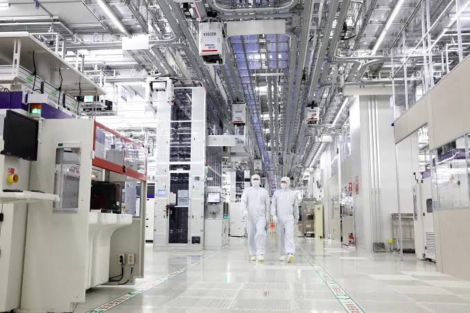

Every time a company announces a new semiconductor factory, the headline almost always includes a staggering price tag. $10 billion. $20 billion. $50 billion. Some projects now stretch beyond $100 billionmaking them among the most expensive industrial investments in history.
At first glance, it seems impossible that a factory—a building with walls, pipes, and machines—could cost more than airports, skyscrapers, or even entire sports stadiums. But here’s the surprising truth: the building itself isn’t what makes a semiconductor fab so expensive.
Most of the money goes into the incredibly advanced machines inside the facility, supported by engineering systems that push the limits of modern science. From extreme ultraviolet (EUV) lithography systems costing hundreds of millions of dollars each to cleanrooms cleaner than hospital operating theaters, every aspect of a chip factory is built with astonishing precision.
Here’s why semiconductor factories have become some of the most expensive facilities humans have ever constructed.
Credits: Construction Physics
The Factory Is Expensive—But the Machines Are Even More Expensive
When people imagine a semiconductor factory, they usually picture a massive industrial building stretching across hundreds of acres. While constructing such a facility certainly isn’t cheap, it represents only a small fraction of the total investment.
In a modern semiconductor fab, around 70% to 80% of the total cost goes toward manufacturing equipment. The remaining portion covers construction, utilities, cleanrooms, and supporting infrastructure.
This means that in a $20 billion facility, roughly $14–16 billion may be spent purely on machinery.
Take Samsung’s Taylor, Texas, project as an example. While the company committed over $17 billion to the project, only a portion is allocated to construction. The majority is dedicated to the specialized manufacturing tools required to produce advanced chips.
These aren’t ordinary industrial machines—they’re among the most sophisticated pieces of engineering ever built.
Lithography Machines Are Worth Hundreds of Millions
If semiconductor manufacturing had a “star player,” it would be the lithography machine.
Lithography is the process of projecting microscopic circuit patterns onto silicon wafers. These patterns eventually become the billions of transistors inside processors, graphics cards, AI chips, and smartphone processors.
Modern chips are so tiny that manufacturers now rely on Extreme Ultraviolet (EUV) lithographya technology that only one company—ASML in the Netherlands—can currently produce at scale.
Each newest-generation EUV machine costs approximately $380 million.
To put that into perspective:
- One EUV machine costs more than many commercial airplanes.
- It weighs over 180 tons.
- It contains more than 100,000 individual components.
- Transporting one machine requires dozens of shipping containers and months of installation.
And one machine isn’t enough.
A cutting-edge fab needs several EUV systems, meaning lithography equipment alone can represent billions of dollars in investment.
Building the Machines Takes Years
Money alone isn’t enough to build a semiconductor plant.
Even after investing billions, manufacturers often wait years for critical equipment to arrive.
ASML only produces a limited number of EUV systems every year because the machines are extraordinarily difficult to manufacture. Thousands of suppliers contribute components that must meet almost impossible precision standards.
As a result, governments and chipmakers compete not just for funding—but also for production slots.
This equipment bottleneck explains why many semiconductor projects take years before production actually begins.
Hundreds of Specialized Machines Work Together
Lithography may receive the attention, but it is only one step in semiconductor manufacturing.
Producing an advanced chip requires hundreds of manufacturing stages involving dozens of different machine types.
These include:
- Etching systems that carve microscopic structures into silicon
- Deposition machines that add ultra-thin material layers
- Ion implantation equipment
- Chemical polishing tools
- Inspection systems capable of identifying defects measured in nanometers
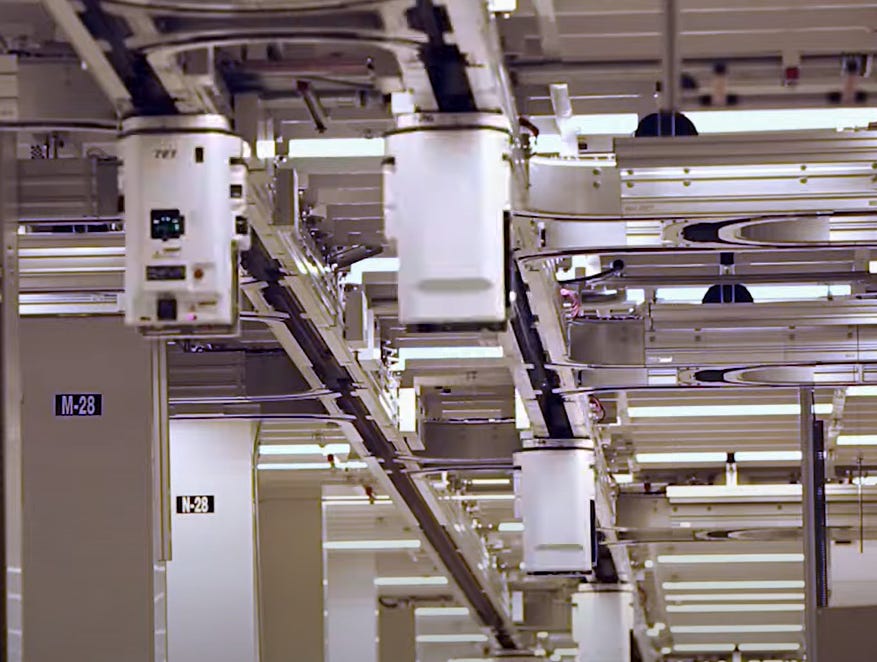
- Automated robotic wafer transport systems
Each category costs hundreds of millions—or even billions—across an entire production line.
Every tool must operate with extraordinary precision because a tiny defect can ruin an entire wafer containing hundreds of valuable chips.
Cleanrooms Cost More Than Most Buildings
One of the biggest surprises about semiconductor manufacturing is that much of the construction budget isn’t spent on walls or roofs.
Instead, it goes toward creating one of the cleanest environments on Earth.
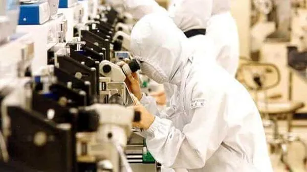
A semiconductor cleanroom is designed to remove virtually every dust particle from the air.
Why?
Because modern transistors are measured in nanometers.
A single dust particle can be hundreds of times larger than the features being printed onto a chip.
Even something invisible to the human eye could destroy an entire production batch.
The world’s most advanced fabs operate at ISO Class 1allowing only an incredibly small number of airborne particles in each cubic meter of air.
Maintaining that level of cleanliness requires:
- Ceiling-wide HEPA and ULPA filtration systems
- Constant positive air pressure
- Highly controlled airflow
- Temperature regulation accurate to fractions of a degree
- Humidity control
- Specialized protective clothing for workers
Building these systems costs billions before the first chip is ever produced.
Credits: Mint
Even the Floor Cannot Vibrate
Imagine trying to draw a perfect line while standing in an earthquake.
That’s essentially what semiconductor manufacturing would be like if factory floors vibrated.
Lithography machines work with incredible precision, aligning circuit patterns measured in billionths of a meter.
Even tiny vibrations caused by nearby traffic, heavy equipment, or footsteps can introduce errors.
To prevent this, fabs are engineered with vibration isolation systems.
Massive concrete foundations are mechanically separated from surrounding structures.
Some equipment sits on specially designed floating platforms that absorb microscopic movement.
Engineers carefully monitor vibration levels because movement measured in just a few micrometers per second can affect chip production.
In many ways, building a semiconductor factory resembles constructing a scientific laboratory rather than a traditional industrial plant.
Credits: Construction Physics
Ultra-Pure Water Is Essential
Water plays an enormous role in semiconductor manufacturing.
Throughout production, wafers are repeatedly cleaned between processing steps.
However, ordinary tap water isn’t remotely clean enough.
Instead, fabs require ultra-pure waterwhich contains almost no minerals, bacteria, particles, or chemical contaminants.
A single advanced semiconductor facility may consume around 10 million gallons of ultra-pure water every day.
Producing that water is itself an expensive engineering process involving multiple purification stages.
Ironically, creating ultra-pure water also wastes significant amounts of water during filtration.
As semiconductor manufacturing expands worldwide, securing reliable water supplies has become one of the biggest challenges for new factory locations.
Semiconductor Fabs Consume Enormous Amounts of Electricity
Electricity represents another major operating expense.
Unlike many factories that periodically slow production, semiconductor fabs often run continuously.
The machinery cannot simply be turned on and off without affecting production.
A large fab can consume roughly 100 megawatt-hours of electricity every hourmaking it one of the most energy-intensive industrial facilities in operation.
This power supports:
- Lithography systems
- Vacuum pumps
- Lasers
- Air filtration
- Water purification
- Cooling systems
- Robotics
- Data centers controlling production
Companies such as TSMC have become some of the largest electricity consumers in the regions where they operate.
Reliable energy infrastructure is now a critical requirement before any semiconductor plant can be built.
The Cost of Building Chip Factories Keeps Rising
The semiconductor industry follows an observation often referred to as Rock’s Law.
It suggests that the cost of building a cutting-edge semiconductor manufacturing facility roughly doubles every four years.
In the early 1970s, a new semiconductor plant could be built for only a few million dollars.
Today, the world’s leading fabs routinely exceed $20 billionwhile entire manufacturing campuses now approach or surpass $100 billion.
The reason is simple.
Every new generation of chips demands:
- Smaller transistors
- More advanced equipment
- Better cleanrooms
- Higher precision
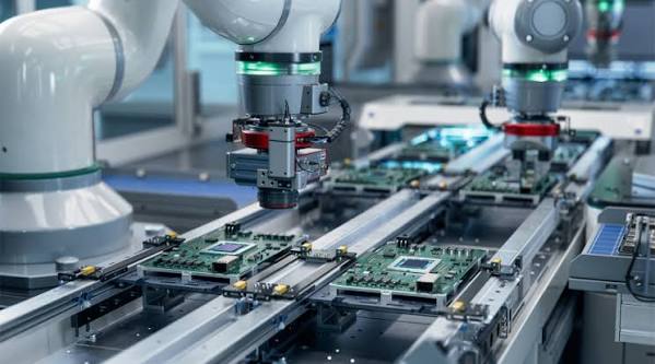
- More automation
- Larger research budgets
As chips become more powerful, the factories required to build them become exponentially more expensive.
Credits: Manufacturing Today
Governments Now Help Pay the Bill
Semiconductor factories have become so expensive that even the world’s largest technology companies rarely finance them entirely on their own.
Governments increasingly view semiconductor production as a matter of national security rather than simply industrial development.
Recent global chip shortages demonstrated how dependent modern economies are on semiconductor supply.
Everything from smartphones and automobiles to military equipment, AI systems, medical devices, and cloud computing depends on advanced chips.
As a result, countries have launched major incentive programs.
The United States introduced the CHIPS and Science Act, providing billions of dollars in grants and tax incentives to encourage domestic manufacturing.
Europe, Japan, South Korea, India, and several other nations have launched similar initiatives aimed at attracting chipmakers.
Instead of competing only on labor costs or taxes, countries now compete by helping finance the construction of semiconductor fabs themselves.
The World’s Most Advanced Factories
Today’s semiconductor factories are unlike any manufacturing facilities that came before them.
They combine physics, chemistry, robotics, artificial intelligence, precision engineering, and advanced manufacturing under one roof.
Every chip inside your smartphone, gaming console, laptop, electric vehicle, or AI server begins life inside one of these highly controlled environments.
The billions spent on semiconductor fabs aren’t simply paying for a building—they’re funding some of the most sophisticated engineering achievements ever created.
As artificial intelligence, autonomous vehicles, quantum computing, and next-generation electronics continue to advance, demand for cutting-edge chips will only increase. That means the race to build bigger, smarter, and even more expensive semiconductor factories is far from over.
The next trillion-dollar technology revolution won’t begin in a flashy office or a software lab. It will begin inside an ultra-clean factory where machines worth hundreds of millions of dollars quietly manufacture the tiny chips powering the modern world.

Comments are closed.